Electrical property refers to the response of a material to an applied electric field. One of the principal characteristics of materials is their ability (or lack of ability) to conduct electrical current. Indeed, materials are classified by this property. That is, they are divided into conductors, semiconductors, and nonconductors.
Electrical Conductivity of Materials
Electrical conductivity and its converse, electrical resistivity, is a fundamental property of a material that quantifies how it conducts the flow of electric current. Electrical conductivity or specific conductance is the reciprocal of electrical resistivity. The symbol for electrical conductivity is κ (kappa), and also σ (sigma) or γ (gamma). The SI unit of electrical conductivity is siemens per meter (S/m). A high conductivity indicates a material that readily allows the flow of electric current. Note that electrical resistivity is not the same as electrical resistance. Electrical resistance is expressed in Ohms. While resistivity is a material property, resistance is the property of an object.
Conductors – Semiconductors – Resistors
Substances in which electricity can flow are called conductors. Conductors are made of high-conductivity materials such as metals, particularly copper and aluminium.
On the other hand, insulators are made of various materials depending on factors such as the desired resistance.
Semiconductors are inorganic or organic materials that can control their conduction depending on chemical structure, temperature, illumination, and the presence of dopants. The name semiconductor comes from the fact that these materials have electrical conductivity between a metal, like copper, gold, etc., and an insulator, like glass. They have an energy gap of less than 4eV (about 1eV). In solid-state physics, this energy gap or band gap is an energy range between the valence and conduction bands where electron states are forbidden. In contrast to conductors, electrons in a semiconductor must obtain energy (e.g., from ionizing radiation) to cross the band gap and reach the conduction band.
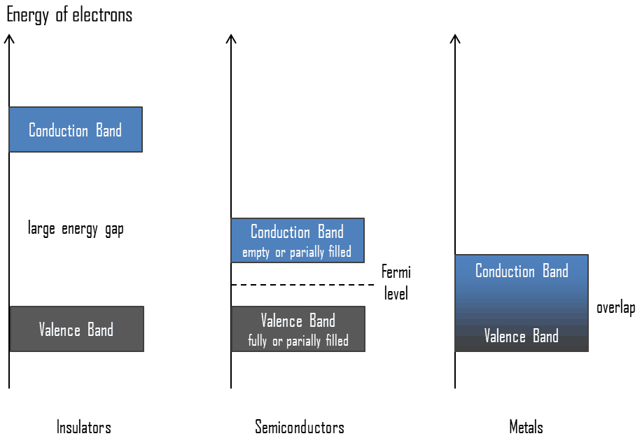
To understand the difference between metals, semiconductors, and electrical insulators, we have to define the following terms from solid-state physics:
 Valence Band. In solid-state physics, the valence band and conduction band are the bands closest to the Fermi level and thus determine the electrical conductivity of the solid. In electrical insulators and semiconductors, the valence band is the highest range of electron energies in which electrons are normally present at absolute zero temperature. For example, a silicon atom has fourteen electrons. In the ground state, they are arranged in the electron configuration [Ne]3s23p2. Four of these are valence electrons, occupying the 3s orbital and two of the 3p orbitals. The distinction between the valence and conduction bands is meaningless in metals because conduction occurs in one or more partially filled bands that take on the properties of both the valence and conduction bands.
- Conduction Band. In solid-state physics, the valence band and conduction band are the bands closest to the Fermi level and thus determine the electrical conductivity of the solid. The conduction band is the lowest range of vacant electronic states in electrical insulators and semiconductors. On a graph of the electronic band structure of a material, the valence band is located below the Fermi level, while the conduction band is above it. In semiconductors, electrons may reach the conduction band when they are excited, for example, by ionizing radiation (i.e., they must obtain energy higher than Egap). For example, diamond is a wide-bandgap semiconductor (Egap = 5.47 eV) with high potential as an electronic device material in many devices. On the other side, germanium has a small band gap energy (Egap = 0.67 eV), which requires operating the detector at cryogenic temperatures. The distinction between the valence and conduction bands is meaningless in metals because conduction occurs in one or more partially filled bands that take on the properties of both the valence and conduction bands.
- Band Gap. In solid-state physics, the energy gap or the band gap is an energy range between the valence band and conduction band where electron states are forbidden. In contrast to conductors, electrons in a semiconductor must obtain energy (e.g., from ionizing radiation) to cross the band gap and reach the conduction band. Band gaps are naturally different for different materials. For example, diamond is a wide-bandgap semiconductor (Egap = 5.47 eV) with high potential as an electronic device material in many devices. On the other side, germanium has a small band gap energy (Egap = 0.67 eV), which requires operating the detector at cryogenic temperatures.
- Fermi Level. The term “Fermi level” comes from Fermi-Dirac statistics, which describes a distribution of particles over energy states in systems consisting of fermions (electrons) that obey the Pauli exclusion principle. Since they cannot exist in identical energy states, Fermi level is the term used to describe the top of the collection of electron energy levels at absolute zero temperature. The Fermi level is the surface of the Fermi sea at absolute zero, where no electrons will have enough energy to rise above the surface. In metals, the Fermi level lies in the hypothetical conduction band giving rise to free conduction electrons. In semiconductors, the position of the Fermi level is within the band gap, approximately in the middle of the band gap.
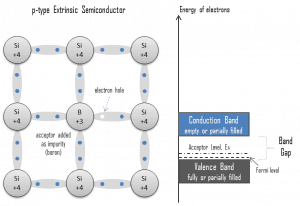 Electron-hole Pair. In semiconductors, free charge carriers are electrons and electron holes(electron-hole pairs). The excitation of electrons creates electrons and holes from the valence band to the conduction band. An electron-hole (often simply called a hole) is the lack of an electron at a position where one could exist in an atom or atomic lattice. It is one of the two types of charge carriers responsible for creating an electric current in semiconducting materials. Since, in a normal atom or crystal lattice, the negative charge of the electrons is balanced by the positive charge of the atomic nuclei, the absence of an electron leaves a net positive charge at the hole’s location. As electrons leave their positions, positively charged holes can move from atom to atom in semiconducting materials. When an electron meets with a hole, they recombine, and these free carriers effectively vanish. The recombination means an electron that has been excited from the valence band to the conduction band falls back to the empty state in the valence band, known as the holes.