In the physics of semiconductors, an electron donor is a dopant atom (impurity) that, when added to a semiconductor, can form an n-type semiconductor. An electron acceptor is a dopant atom (impurity) that, when added to a semiconductor, can form a p-type semiconductor. The process of adding controlled impurities to a semiconductor is known as semiconductor doping, and this process changes an intrinsic semiconductor to an extrinsic semiconductor. Increasing dopant density increases conductivity for both types of donor or acceptor atoms.
n-type Semiconductors
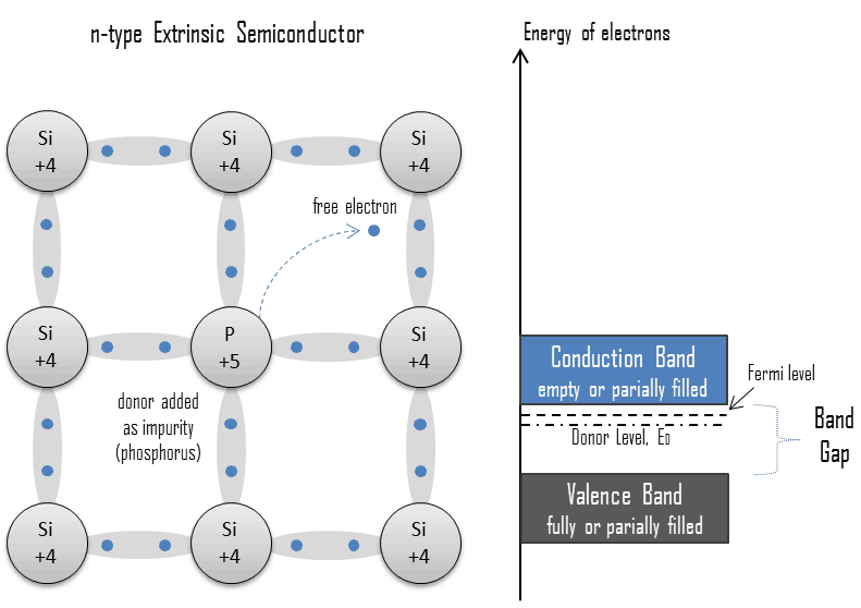 An extrinsic semiconductor doped with electron donor atoms is called an n-type semiconductor because most charge carriers in the crystal are negative electrons. Since silicon is a tetravalent element, the normal crystal structure contains 4 covalent bonds from four valence electrons. In silicon, the most common dopants are group III and group V elements. Group V elements (pentavalent) have five valence electrons, allowing them to act as donors. That means adding these pentavalent impurities such as arsenic, antimony, or phosphorus contributes to free electrons, greatly increasing the conductivity of the intrinsic semiconductor. For example, a silicon crystal doped with boron (group III) creates a p-type semiconductor, whereas a crystal doped with phosphorus (group V) results in an n-type semiconductor.
The conduction electrons are completely dominated by the number of donor electrons. Therefore:
The total number of conduction electrons is approximately equal to the number of donor sites, n≈ND.
The charge neutrality of semiconductor material is maintained because excited donor sites balance the conduction electrons. The net result is that the number of conduction electrons increases while the number of holes is reduced. The imbalance of the carrier concentration in the respective bands is expressed by the different absolute number of electrons and holes. Electrons are majority carriers, while holes are minority carriers in n-type material.
p-type Semiconductors
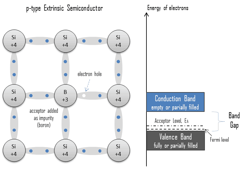 An extrinsic semiconductor doped with electron acceptor atoms is called a p-type semiconductor because most charge carriers in the crystal are electron holes (positive charge carriers). The pure semiconductor silicon is a tetravalent element, and the normal crystal structure contains 4 covalent bonds from four valence electrons. In silicon, the most common dopants are group III and group V elements. Group III elements (trivalent) all contain three valence electrons, causing them to function as acceptors when used to dope silicon. When an acceptor atom replaces a tetravalent silicon atom in the crystal, a vacant state (an electron-hole) is created. An electron-hole (often simply called a hole) is the lack of an electron at a position where one could exist in an atom or atomic lattice. It is one of the two charge carriers responsible for creating an electric current in semiconducting materials. These positively charged holes can move from atom to atom in semiconducting materials as electrons leave their positions. Adding trivalent impurities such as boron, aluminum, or gallium to an intrinsic semiconductor creates these positive electron holes in the structure. For example, a silicon crystal doped with boron (group III) creates a p-type semiconductor, whereas a crystal doped with phosphorus (group V) results in an n-type semiconductor.
The number of electron holes is completely dominated by the number of acceptor sites. Therefore:
The total number of holes is approximately equal to the number of donor sites, p ≈ NA.
The charge neutrality of this semiconductor material is also maintained. The net result is that the number of electron holes is increased while the number of conduction electrons is reduced. The imbalance of the carrier concentration in the respective bands is expressed by the different absolute number of electrons and holes. Electron holes are majority carriers, while electrons are minority carriers in p-type material.