An extrinsic semiconductor, or doped semiconductor, is a semiconductor that was intentionally doped to modulate its electrical, optical, and structural properties. In the case of semiconductor detectors of ionizing radiation, doping is the intentional introduction of impurities into an intrinsic semiconductor for the purpose of changes in their electrical properties. Therefore, intrinsic semiconductors are also known as pure semiconductors or i-type semiconductors.
Adding a small percentage of foreign atoms in the regular crystal lattice of silicon or germanium produces dramatic changes in their electrical properties since these foreign atoms incorporated into the crystal structure of the semiconductor provide free charge carriers (electrons or electron holes) in the semiconductor. In an extrinsic semiconductor, these foreign dopant atoms in the crystal lattice mainly provide the charge carriers that carry electric current through the crystal. In general, two types of dopant atoms result in two types of extrinsic semiconductors. These dopants that produce the desired controlled changes are classified as either electron acceptors or donors, and the corresponding doped semiconductors are known as:
- n-type Semiconductors.
- p-type Semiconductors.
_______________
 In semiconductors, free charge carriers are electrons and electron holes (electron-hole pairs). Electrons and holes are created by exciting electrons from the valence band to the conduction band. An electron-hole (often simply called a hole) is the lack of an electron at a position where one could exist in an atom or atomic lattice. It is one of the two charge carriers responsible for creating an electric current in semiconducting materials. Since, in a normal atom or crystal lattice, the negative charge of the electrons is balanced by the positive charge of the atomic nuclei, the absence of an electron leaves a net positive charge at the hole’s location. As electrons leave their positions, positively charged holes can move from atom to atom in semiconducting materials. When an electron meets with a hole, they recombine, and these free carriers effectively vanish. The recombination means an electron that has been excited from the valence band to the conduction band falls back to the empty state in the valence band, known as the holes.
The conductivity of a semiconductor can be modeled in terms of the band theory of solids. The band model of a semiconductor suggests that at ordinary temperatures, there is a finite possibility that electrons can reach the conduction band and contribute to electrical conduction. In the semiconductor, free charge carriers (electron-hole pairs) are created by the excitation of electrons from the valence band to the conduction band. This excitation left a hole in the valence band, which behaves as a positive charge, and an electron-hole pair is created. Holes can sometimes be confusing as they are not physical particles in the way that electrons are. Rather they are the absence of an electron in an atom. Holes can move from atom to atom in semiconducting materials as electrons leave their positions.
Charge Carriers in Extrinsic Semiconductors
The number of charge carriers of pure semiconductors at a certain temperature is determined by the material’s properties instead of the number of impurities. Note that a 1 cm3 sample of pure germanium at 20 °C contains about 4.2×10²² atoms but also contains about 2.5 x 10¹³ free electrons and 2.5 x 10¹³ holes. These charge carriers are produced by thermal excitation. In intrinsic semiconductors, the number of excited electrons and the number of holes are equal: n = p. Electrons and holes are created by the excitation of an electron from the valence band to the conduction band. An electron-hole (often simply called a hole) is the lack of an electron at a position where one could exist in an atom or atomic lattice. This equality may even be the case after doping the semiconductor, though only if it is doped with both donors and acceptors equally. In this case, n = p still holds, and the semiconductor remains intrinsic, though doped. Adding 0.001% of arsenic (an impurity) donates an extra 1017 free electrons in the same volume, and the electrical conductivity is increased by a factor of 10,000. The signal-to-noise ratio (S/N) would be even smaller in doped material. Because germanium has a relatively low band gap, these detectors must be cooled to reduce the thermal generation of charge carriers (thus reverse leakage current) to an acceptable level. Otherwise, leakage current-induced noise destroys the energy resolution of the detector.
Charge Carriers in n-type Semiconductors
In the n-type semiconductor, the conduction electrons are completely dominated by the number of donor electrons. Therefore:
The total number of conduction electrons is approximately equal to the number of donor sites, n≈ND.
The charge neutrality of semiconductor material is maintained because excited donor sites balance the conduction electrons. The net result is that the number of conduction electrons increases while the number of holes is reduced. The imbalance of the carrier concentration in the respective bands is expressed by the different absolute number of electrons and holes. Electrons are majority carriers, while holes are minority carriers in n-type material.
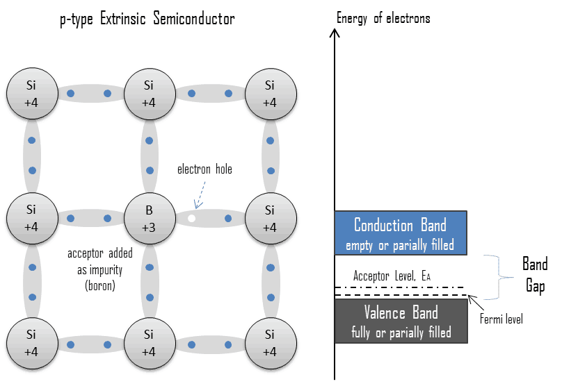
Charge Carriers in p-type Semiconductors
In the p-type semiconductor, the number of electron holes is completely dominated by the number of acceptor sites. Therefore:
The total number of holes is approximately equal to the number of donor sites, p ≈ NA.
The charge neutrality of this semiconductor material is also maintained. The net result is that the number of electron holes is increased while the number of conduction electrons is reduced. The imbalance of the carrier concentration in the respective bands is expressed by the different absolute number of electrons and holes. Electron holes are majority carriers, while electrons are minority carriers in p-type material.