n-type Semiconductors
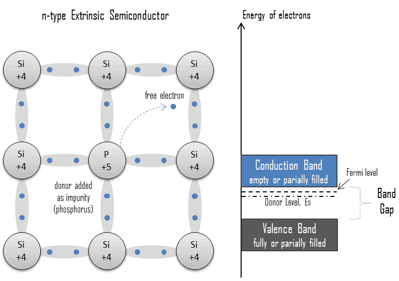 An extrinsic semiconductor doped with electron donor atoms is called an n-type semiconductor because most charge carriers in the crystal are negative electrons. Since silicon is a tetravalent element, the normal crystal structure contains 4 covalent bonds from four valence electrons. In silicon, the most common dopants are group III and group V elements. Group V elements (pentavalent) have five valence electrons, allowing them to act as donors. That means adding these pentavalent impurities such as arsenic, antimony, or phosphorus contributes to free electrons, greatly increasing the conductivity of the intrinsic semiconductor. For example, a silicon crystal doped with boron (group III) creates a p-type semiconductor, whereas a crystal doped with phosphorus (group V) results in an n-type semiconductor.
The conduction electrons are completely dominated by the number of donor electrons. Therefore:
The total number of conduction electrons is approximately equal to the number of donor sites, n≈ND.
The charge neutrality of semiconductor material is maintained because excited donor sites balance the conduction electrons. The net result is that the number of conduction electrons increases while the number of holes is reduced. The imbalance of the carrier concentration in the respective bands is expressed by the different absolute number of electrons and holes. Electrons are majority carriers, while holes are minority carriers in n-type material.
Donor Level
From the energy gap viewpoint, such impurities “create” energy levels in the band gap close to the conduction band so that electrons can be easily excited from these levels into the conduction band. The electrons are said to be the “majority carriers” for current flow in an n-type semiconductor. This shifts the effective Fermi level to a point about halfway between the donor levels and the conduction band. Fermi level is the term used to describe the top of the collection of electron energy levels at absolute zero temperature. The Fermi level is the surface of the Fermi sea at absolute zero, where no electrons will have enough energy to rise above the surface. In pure semiconductors, the position of the Fermi level is within the band gap, approximately in the middle of the band gap.