 In semiconductors, free charge carriers are electrons and electron holes (electron-hole pairs). Electrons and holes are created by the excitation of an electron from the valence band to the conduction band. An electron-hole (often simply called a hole) is the lack of an electron at a position where one could exist in an atom or atomic lattice. It is one of the two types of charge carriers that are responsible for creating an electric current in semiconducting materials. Since, in a normal atom or crystal lattice, the negative charge of the electrons is balanced by the positive charge of the atomic nuclei, the absence of an electron leaves a net positive charge at the hole’s location. As electrons leave their positions, positively charged holes can move from atom to atom in semiconducting materials. When an electron meets with a hole, they recombine, and these free carriers effectively vanish. The recombination means an electron that has been excited from the valence band to the conduction band falls back to the empty state in the valence band, known as the holes.
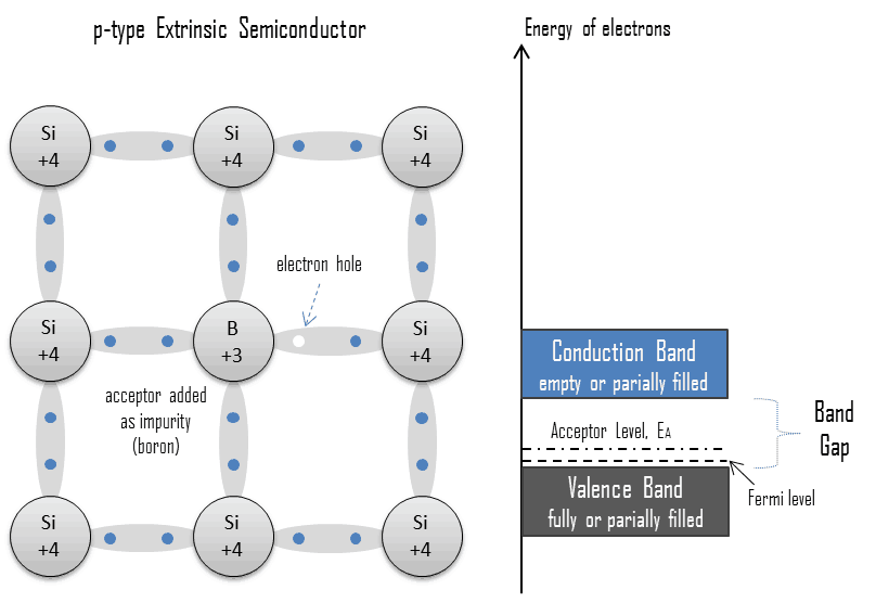
The conductivity of a semiconductor can be modeled in terms of the band theory of solids. The band model of a semiconductor suggests that at ordinary temperatures, there is a finite possibility that electrons can reach the conduction band and contribute to electrical conduction. In the semiconductor, free charge carriers (electron-hole pairs) are created by the excitation of an electron from the valence band to the conduction band. This excitation left a hole in the valence band, which behaves as a positive charge, and an electron-hole pair is created. Holes can sometimes be confusing as they are not physical particles in the way that electrons are. Rather they are the absence of an electron in an atom. Holes can move from atom to atom in semiconducting materials as electrons leave their positions.
Electron Excitation in Semiconductors
Energy for the excitation can be obtained in different ways.
Thermal Excitation
Electron-hole pairs are also constantly generated from thermal energy without any external energy source. Thermal excitation does not require any other form of starting impulse. This phenomenon also occurs at room temperature. It is caused by impurities, structure lattice irregularities, or dopants. It strongly depends on the Egap (a distance between valence and conduction band), so that for lower Egap, the number of thermally excited charge carriers increases. Since thermal excitation results in the detector noise, active cooling is required for some types of semiconductors (e.g., germanium). Detectors based on silicon have sufficiently low noise even at room temperature. This is caused by the large band gap of silicon (Egap= 1.12 eV), which allows us to operate the detector at room temperature, but cooling is preferred to reduce noise.
Optical Excitation
Note that the energy of a single photon of the visible light spectrum is comparable with these band gaps. Photons of wavelengths 700 nm – 400 nm have energies of 1.77 eV to 3.10 eV. As a result, visible light can also excite electrons to the conduction band, which is the principle of photovoltaic panels that generate electric currents.
Excitation by Ionizing Radiation
Electrons may reach the conduction band when they are excited by ionizing radiation (i.e., they must obtain energy higher than Egap). In general, heavy charged particles transfer energy mostly by:
- Excitation. The charged particle can transfer energy to the atom, raising electrons to higher energy levels.
- Ionization. Ionization can occur when the charged particle has enough energy to remove an electron, creating ion pairs in surrounding matter.
A convenient variable that describes the ionization properties of the surrounding medium is the stopping power, and the classical expression describing the specific energy loss is the Bethe formula. For alpha particles and heavier particles, the stopping power of most materials is very high for heavy charged particles, and these particles have very short ranges.
In addition to these interactions, beta particles lose energy through a radiative process known as the bremsstrahlung. From classical theory, when a charged particle is accelerated or decelerated, it must radiate energy, and the deceleration radiation is known as the bremsstrahlung (“braking radiation”).
Photons (gamma rays and X-rays) can ionize atoms directly (despite they are electrically neutral) through the Photoelectric effect and the Compton effect, but secondary (indirect) ionization is much more significant. Although many possible interactions are known, there are three key interaction mechanisms with the matter.
In all cases, a particle of ionizing radiation deposits a portion of its energy along its path. Particle passing through the detector ionizes the atoms of the semiconductor, producing the electron-hole pairs. For example, the typical thickness of a silicon detector is about 300 µm, so the number of generated electron-hole pairs by a minimum ionizing particle (MIP) passing perpendicular through the detector is about 3.2 x 10⁴. This value is minor compared to the total number of free carriers in an intrinsic semiconductor with a surface of 1 cm2 and the same thickness. Note that a sample of pure germanium at 20 °C contains about 1.26×10²¹ atoms but also contains 7.5 x 10¹¹ free electrons and 7.5 x 10¹¹ holes constantly generated from thermal energy. As can be seen, the signal-to-noise ratio (S/N) would be minimal. Adding 0.001% of arsenic (an impurity) donates an extra 1015 free electrons in the same volume, and the electrical conductivity is increased by a factor of 10,000. The signal-to-noise ratio (S/N) would be even smaller in doped material. Cooling the semiconductor is one way to lower this ratio.
Improvement can be achieved by using a reverse-bias voltage to the P-N junction to deplete the detector of free carriers, which is the principle of most silicon radiation detectors. In this case, a negative voltage is applied to the p-side and positive to the second one. Holes in the p-region are attracted from the junction towards the p contact and similarly for electrons and the n contact.